つちだ ひでかず
Hidekazu Tsuchida
◆第58回(令和7(2025)年度)市村賞 市村産業賞 貢献賞を受賞しました。◆
第58回 市村産業賞 貢献賞
◆第50回(2023年度)岩谷直治記念賞を受賞しました。◆
ORCiD: https://orcid.org/0009-0009-9753-9929
Scopus Author ID: 25032218200
ResearcherID: ISB-3157-2023
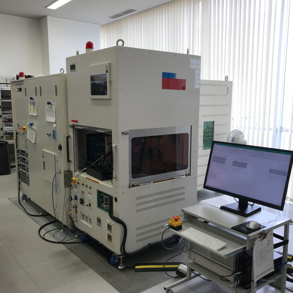
大容量SiCパワー半導体素子に向けたエピタキシャル結晶成長技術の開発 -低マイクロパイプ密度,厚膜・高純度4H-SiCエピタキシャル単結晶膜の形成-
Development of epitaxial growth techniques for high-power SiC semiconductor devices
2003年04月
厚膜 SiC 単結晶成長ならびに SiC 表面吸着質・酸化膜評価に関する研究
Study on growth of thick SiC epitaxial layers and characterization of surface adsorbates and oxides on SiC
1999年05月
パワー半導体素子の現状と高性能化の課題に関する調査-半導体開閉装置への適用-
SURVEY ON PRESENT STATUS OF POWER SEMICONDUCTOR FOR DEVICES AND HIGH-PERFOERMANCE TECHNIQUE-APPLICATION TO SOLID-STATE SWITCHGEAR-
1994年05月
SiC/絶縁膜界面制御技術の開発
Development of control technology for the interface of SiC/insulation film
2011年05月
第一原理計算によるSiC熱酸化シミュレーション手法の開発
Developement of SiC thermal oxidation simulation by first-principles calculation
2006年06月
SiC単結晶膜中欠陥の高分解能非破壊観察法の開発
Development of high-resolution and non-destructive observation techniques on SiC epilayers
2005年09月
[主な学会発表、講演]
1. <Plenary invited talk> H. Tsuchida, “4H-SiC as material for electricity infrastructure”, International Conference on Silicon carbide and Related Materials 2025 (ICSCRM2025), Busan, Korea, 2025.9.
2. <Invited talk> H. Tsuchida, S. Asada, F. Fujie, “Analysis of stacking faults and formation mechanism of basal plane dislocations in 4H-SiC”, ACCGE24/OMVPE22, Stevenson, Washington, USA, 2025.7.
3. <Plenary invited talk> H. Tsuchida, “Growth and defect characterization of 4H-SiC bulk crystals and epilayers for high-voltage devices”, The 8th International Symposium on Wide Bandgap Semiconductor 2024 (WBGS2024), Busan, Korea, 2024.11.
4. <Invited talk> H. Tsuchida, T. Kanda, “Progress in fast 4H-SiC crystal growth and defect reduction by high-temperature gas-source method”, Pacific Rim Meeting on Electrochemical and Solid state Science 2024 (PRiME2024), Honolulu, HI, USA, 2024.10.
5. <Plenary invited talk> H. Tsuchida, “Defect characterization and control for suppression
of bipolar degradation in 4H-SiC power devices”, 20th International Conference on Defects Recognition, Imaging and Physics in Semiconductors, Stony Brook, NY, USA, 2024.8.
6. <招待講演> 土田秀一、宇治原徹、原田俊太、沓掛健太朗、村山健太、高石将輝、「SiCバルク結晶製造技術の革新に向けたプロセスインフォマティクス技術の研究」、電気情報通信学会総合大会、広島大学、広島、2024.3.
7. <Invited talk> K. Murata, T. Miyazawa, H. Tsuchida, “Carrier lifetime control for designing buffer and drift layers in 4H-SiC devices”, International Conference on Silicon carbide and Related Materials 2022 (ICSCRM2022), Davos, Switzerland, 2022.9.
8. <Invited talk> H. Tsuchida, I. Kamata, N. Hoshino, K. Murata, “Recent progress in 4H-SiC CVD growth and defect control”, 13th European Conference on Silicon Carbide and Related Materials 2020・2021 (ECSCRM2021・2022), Tours, France, 2021.10.
9. <Invited talk> H. Tsuchida, K. Murata, T. Tawara, M. Miyazato, T. Miyazawa, K. Maeda, “Suppression of bipolar degradation in 4H-SiC power devices by carrier lifetime control”, 65th International Electron Devices Meeting (IEDM 2019), San Francisco, CA, USA, 2019.12.
10. <招待講演> 土田秀一、村田晃一、宮澤哲哉、鎌田功穂、星乃紀博、「高電圧パワーデバイスに向けた4H-SiC CVD成長技術の進展」、先進パワー半導体分科会第6回講演会、広島国際会議場、広島、2019.12.
→その他主な学会発表・講演リストはこちら
1. 第58回(令和7(2025)年度)市村賞 市村産業賞 貢献賞、深田啓介、百瀬賢治、土田秀一、「パワー半導体用高品質SiCエピウェハーの高生産性製造技術」、2026.3.
2. 第50回(2023年度)岩谷直治記念賞、土田秀一、藤林裕明、伊藤英樹、深田啓介、「高品質SiC単結晶膜の高速製造技術の開発と応用」、2024.3.
3. 応用物理学会論文賞(優秀論文賞)、N. Hoshino, I. Kamata, T. Kanda, Y. Tokuda, H. Kuno, H. Tsuchida, “Reduction in dislocation densities in 4H-SiC bulk crystal grown at high growth rate by high-temperature gas-source method”, 2023.3.
4. SSDM 2019 Poster Award, Y. Tokuda, H. Uehigashi, K. Murata, H. Tsuchida, “Fabrication of 4H-SiC PiN diodes on substrate grown by HTSVD method”, 2019.9.
5. 応用物理学会論文賞(優秀論文賞)、R. Tanuma, M. Nagano, I. Kamata, H. Tsuchida, “Three-dimensional imaging and tilt-angle analysis of dislocations in 4H-SiC by two-photon-excited band-edge photoluminescence”, 2016.9.
6. 電気科学技術奨励賞、中山浩二、石井竜介、土田秀一、「大容量・高耐熱SiCツェナーダイオードの開発」、オーム社、2010.11.
7. 電気学術振興賞論文賞、中山浩二、菅原良孝、石井竜介、土田秀一、鎌田功穂、中村智宣、「4H-SiC pinダイオードの順方向劣化特性と高耐圧少劣化 (000-1)C面4H-SiC pin ダイオード」、電気学会、2010.6.
8. MRS Meeting Outstanding Paper, I. Kamata, H. Tsuchida, W. Vetter, M. Dudley, “High-Resolution X-ray Topography of Dislocations in 4H-SiC Epilayers”, Material Research Society, 2006.9.
9. JJAP 論文賞、I. Kamata, H. Tsuchida, T. Jikimoto, K. Izumi “Influence of 4H-SiC epitaxial growth conditions on micropipe dissociation”、応用物理学会、2004.9.
10. 応用物理学会講演奨励賞、土田秀一、「全反射赤外吸収分光法によるSiC単結晶表面の評価」、応用物理学会、1998.3.
1. General chair of International Conference on Silicon Carbide and Related Materials 2026 (ICSCRM 2026), H. Tsuchida (2025.9-present)
2. 応用物理学会「半導体の結晶成長と加工および評価に関する産学連携委員会」、土田秀一(副委員長: 2023.4.1-現在)
3. International Steering Committee of International Conference on Silicon Carbide and Related Materials (ICSCRM), H. Tsuchida (member: 2022.11-present)
4. International Steering Committee of International Conference on Defects-Recognition, Imaging and Physics in Semiconductor (DRIP), H. Tsuchida (member: 2012.4-present, chair: 2022.9-2024.8)
5. Conference chair of the 19th International Conference on Defects-Recognition, Imaging and Physics in Semiconductor (DRIP XIX), H. Tsuchida (2019.1-2023.10)
6. Technical program committee of International Conference on Silicon Carbide and Related Materials 2025 (ICSCRM 2025), H. Tsuchida (member: 2024.11-present)
7. Technical program committee of International Conference on Silicon Carbide and Related Materials 2024 (ICSCRM 2024), H. Tsuchida (member: 2023.11-2024.10)
8. Technical program committee of International Conference on Silicon Carbide and Related Materials 2023 (ICSCRM 2023), H. Tsuchida (member: 2022.11-2023.9)
9. Technical program committee of 13th European Conference on Silicon Carbide and Related Materials 2020-2021 (ECSCRM 2020/2021), H. Tsuchida (member: 2019.10-2021.10)
10. 日本学術振興会第145委員会「結晶評価と加工」、土田秀一(副委員長: 2018.4-2023.3.31)
11. 応用物理学会先進パワー半導体分科会幹事会、土田秀一(幹事長: 2016.1-2017.12、副幹事長: 2014.1-2015.12)
12. 京都大学卓越大学院「先端光・電子デバイス創成学」、土田秀一(担当者: 2019.4-現在)
13. 第6回パワーデバイスシリコンおよび関連半導体材料に関する研究会、土田秀一(実行委員長: 2017.1-2018.12)
14. IEA 4E Power Electronic Conversion Technology Annex (PECTA), PECTA-experts, H. Tsuchida (member: 2020.10-present)
15. Technical program committee of International Conference on Silicon Carbide and Related Materials 2019 (ICSCRM 2019), H. Tsuchida (chair: 2017.10-2019.10)
16. Technical program committee of International Conference on Silicon Carbide and Related Materials 2017 (ICSCRM 2017), H. Tsuchida (member: 2015.10-2017.9)
17. Technical program committee of International Conference on Silicon Carbide and Related Materials 2015 (ICSCRM 2015), H. Tsuchida (member: 2013.11-2015.10)
18. Program Committee of 2013 International Conference on Solid State Devices and Materials, H. Tsuchida (SSDM 2013), H. Tsuchida (area chair: 2012.10-2013.9)
19. Technical program Committee of International Conference on Silicon Carbide and Related Materials 2013 (ICSCRM 2013), H. Tsuchida (member: 2012.11-2013.10)
20. Technical program committee of International Conference on Silicon Carbide and Related Materials 2011 (ICSCRM 2011), H. Tsuchida (member: 2009.10-2011.9)
21. SiC及び関連ワイドギャップ半導体研究会第17回講演会、土田秀一(実行委員長: 2008.1-2008.12)
[学術論文]
【外部資金獲得】
【特許出願・登録状況】
国内特許出願: 110件、特許登録(特許公報): 93件(2026年3月23日現在)